Metagratings are sparse (typically periodic) arrangements of subwavelength polarizable particles (meta-atoms). Unlike metasurfaces, in which the meta-atoms are dense and closely packed, metagratings do not adhere to the homogenization approximation. Instead, their interaction with incident fields is modeled by considering mutual coupling between individual elements. We design them based on a bottom-up approach: reliable analytical models are formulated, enabling prediction of the currents induced on individual scatterers in response to incoming excitation; these currents act as secondary sources, which give rise to an interference pattern, which can be readily evaluated using the analytical models; to generate a metagrating implementing a given field transformation, we stipulate suitable constraints on the interference pattern (given in terms of a Floquet-Bloch expansion for the periodic structures), and correspondingly resolve the meta-atom distribution and geometry as to satisfy these constraints. Since the analytical model takes into account the actual physical structure of the meta-atoms, the resultant design specifications is in the form of a fabrication-ready layout. This is a tremendous advantage compared to metasurfaces, since there is no need for length optimization in full-wave solvers to engineer the detailed meta-atom configuration. In addition, the metagrating synthesis procedure clearly identifies the minimal required number of degrees of freedom, thus enhances device sparsity and simplicity, as well as rigorously incoprates conductor and dielectric loss effects, boosting up device efficiency.
Beam manipulation
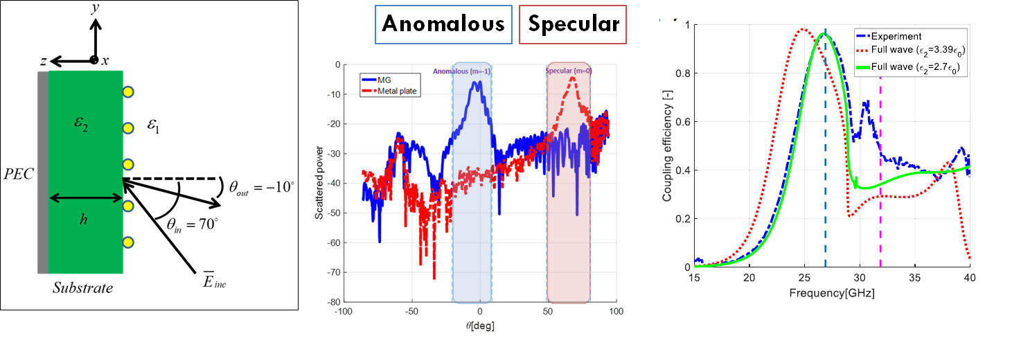
In our work we usually use capacitively loaded wires as meta-atoms, and have developed a complete analytical methodology to design such metagratings using the wire position and capacitor widths as degrees of freedom. The basic idea was extended by us to incorporate a realistic substrate into the model, enabling complete printed-circuit-board (PCB) realization in of a wide-angle perfect anomalous reflector the microwave regime, subsequently verified experimentally.
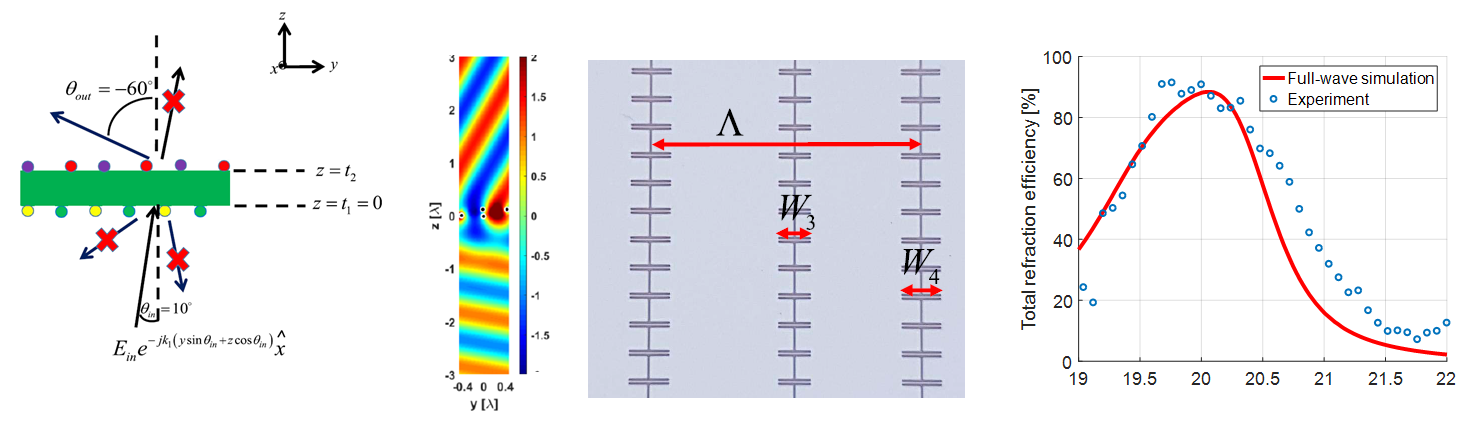
 Adding more degrees of freedom, namely, enabling additional meta-atoms per period with potentially variable horizontal and vertical offsets, we have extended the model to facilitate transmissive field manipulation. The concept was demonstrated experimentally via a prototype implementing wide-angle perfect anomalous refraction.
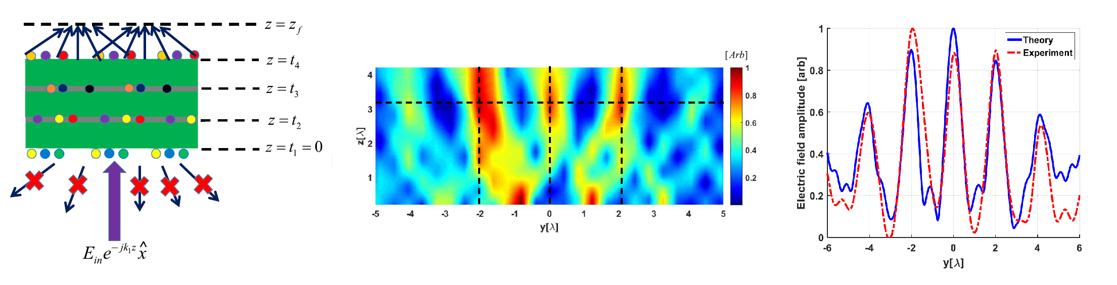
We have continued to evolve this concept of beam-manipulating metagratings, resulting in a general multilayer multielement metagrating model, which can control the amplitude and phase of numerous modes, in both reflection and transmission. We have demonstrated these capabilities with a nonlocal lens array, yielding multiple tight foci at the designated focal plane, the formation of which is facilitated by the entire metagrating.
 Manipulation of guided modes
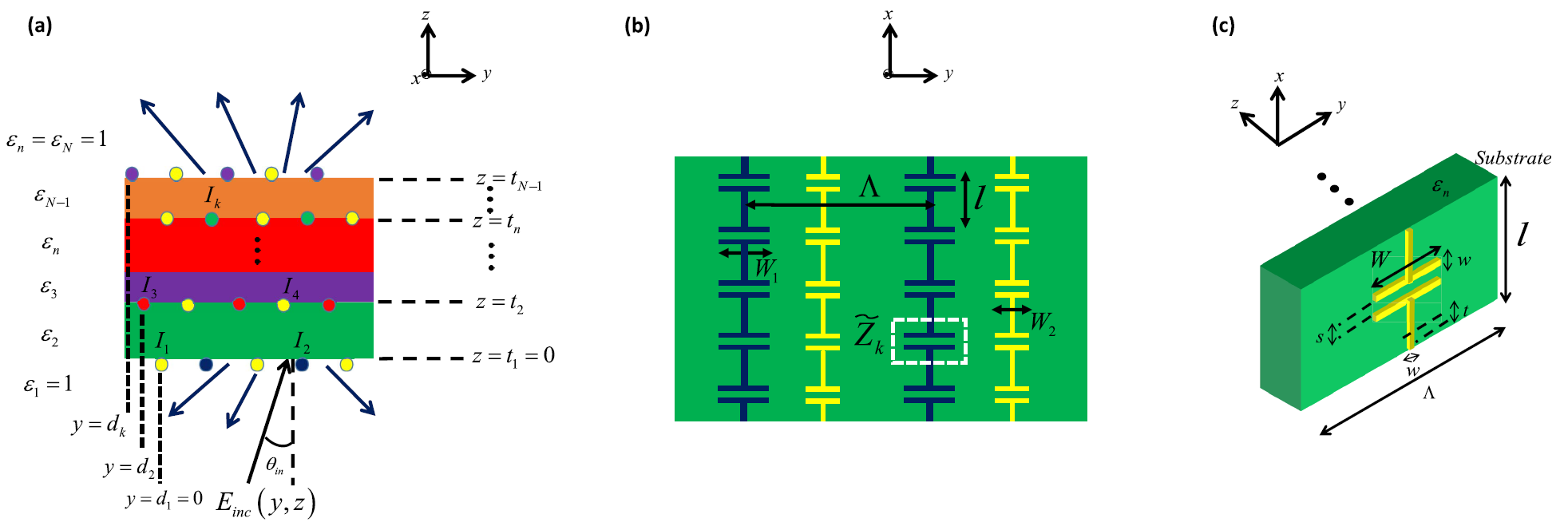
The metagrating synthesis approach is based on modal analysis, deriving the conditions by which a certain set of scatterers (acting as secondary sources) can cause destructive interference for spurious modes, while funneling all of the input power into the desired mode. The resultant powerful methodology, yielding directly fabrication-ready designs of simple and sparse structures with meticulous control over coupling to the various modes, is highly appealing for other electromagnetic scenarios as well. In particular, we have devised metagrating-based solutions to common problems in rectangular waveguides.
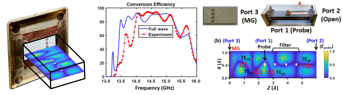
The first problem tackled is mode conversion, useful as a preliminary step prior to power splitting or for increasing channel capacity. In particular, we have extended the metagrating synthesis approach to enable complete power transfer from an incident TE10 mode into a reflected TE20 mode within the waveguide. Harnessing the analogy between beam interaction with a periodic surface and the effective periodicity formed by the metallic walls, we have adapted the analytical formalism to enable perfect mode conversion using a simple PCB termination. The method points out favorable positions for a capacitively loaded wire, the substrate thickness, and the geometry of the load printed capacitor, to facilitate optimal coupling. The resultant fabrication-ready design (in the form of a small PCB card) is manufactured without any further optimization, and characterized using two different setups – S-parameter measurement with a VNA, and radiation pattern characteristics of the open-ended waveguide. Despite being fundamentally different, both measurements excellently agree with each other, pointing out that the fabricated prototype successfully couples more than 90% of the input power into the higher-order mode.
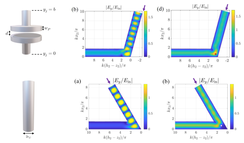
Next, we have looked into another common problem in complex waveguide systems – reflection loss due to bend discontinuity. To mitigate this issue, enabling unitary power transmission across arbitrary waveguide bends, we have analyzed the bend configuration when a single meta-atom is placed at the junction. By expanding the fields into rectangular waveguide modes at the input and output, and radial waveguide modes in the junction, we were able to follow the metagrating design rationale – find those locations where a passive scatterer can be placed as to facilitate destructive interference with the reflected waves, thus completely quenching back reflections. This elegant semianalytical methodology, can be used also to find an approximate geometry for the scatterer (a simple metallic post would suffice many times), therefore providing an efficient path for designing waveguide bend transitions without any geometry deformation or sophisticated numerical optimizations.